EO Modulation Systems
EO Modulation Systems and Applications (EO Modulators)


Conoptics is delivering products in 30 to 60 days. Call now to place your order.
Domestic (800) 748-3349 – International (203) 743-3349
Demands for Wider-Band Beam Modulation Challenge System Designers by Robert F. Enscoe and Richard J. Kocka
Electro-Optic (EO) modulation systems are at the heart of modern optical communication and laser technology. These systems enable precise control over the properties of light, making them indispensable in a wide range of applications, from data recording to advanced spectroscopy. Proper alignment of the optical input is crucial for optimal modulator performance, as misalignment can lead to excess optical power absorption and potential device damage. By leveraging the unique properties of electro-optic materials, EO modulators can manipulate light with exceptional speed and accuracy, paving the way for innovations in both scientific research and commercial technologies. Optical fibers play a key role in integrating EO modulators into fiber-optic systems, facilitating efficient light coupling and signal transmission.
What are Electro-Optic Modulators?
Electro-optic modulators (EOMs) are sophisticated devices designed to control the power, phase, or polarization of light through an electrical control signal. A specific type of EOM, known as phase modulators, alters the phase of a laser beam by applying an electric field to the device. At the core of their operation is the linear electro-optic effect, commonly known as the Pockels effect. By utilizing amplitude and phase modulators, different applications can achieve high-speed optical modulation, precise wavelength coverage, and tailored technical specifications. This phenomenon occurs when an electric field is applied to a nonlinear crystal, causing a change in its refractive index proportional to the field strength. The electric field interacts with the optical mode within the crystal, enabling effective phase modulation and light control. By exploiting this effect, EOMs can modulate an optical signal with high precision and speed. These modulators are integral to various applications, including optical communication systems, where they encode data onto light waves, and in laser technology, where they fine-tune laser beams for specific tasks. The properties of the input beam, such as polarization and alignment, are crucial for achieving effective modulation with electro-optic modulators.
Electro-optic modulation technology has evolved through decades of engineering refinement across research laboratories, telecommunications infrastructure, and precision laser manufacturing environments. Engineers working with EO modulators must consider not only theoretical electro-optic coefficients, but also practical factors such as thermal stability, impedance matching, crystal orientation tolerances, and long-term reliability under sustained optical power loads. Manufacturers with specialized experience in electro-optic components contribute significantly to system performance because subtle design decisions — including electrode geometry, material purity, and mechanical packaging — directly influence modulation bandwidth, insertion loss, and operational stability. Understanding these real-world constraints helps bridge the gap between laboratory theory and deployable optical systems.
Types of Electro-Optic Modulators
Amplitude Modulation
Amplitude modulation is a fundamental technique where the amplitude of a light beam is varied in accordance with an information signal. Amplitude modulators, a specific type of electro-optic modulator, are designed to influence the intensity of laser light. These modulators utilize electro-optical crystals that exhibit a rapid electro-optical effect, allowing them to operate at high modulation frequencies, often reaching into the gigahertz range. One of the key advantages of amplitude modulators is their high optical power stability, which ensures consistent performance. Additionally, they require low modulation voltages and offer high extinction ratios, making them highly efficient for applications that demand precise control over light intensity. Whether in high-speed data transmission or advanced imaging systems, amplitude modulators play a crucial role in enhancing the performance and reliability of optical technologies.
Materials and Configurations of EO Modulators
Electro-optic modulators are engineered from a variety of advanced materials, each selected for its unique electro-optic properties and suitability for specific applications. Among the most widely used are lithium niobate (LiNbO₃), potassium di-deuterium phosphate (KD*P), and beta-barium borate (BBO). These electro-optic crystals are prized for their ability to exhibit a strong electro-optic effect, where the refractive index changes in response to an applied electric field. The choice of electro-optic material directly influences critical performance parameters such as half wave voltage—the voltage required to induce a π phase shift—modulation frequency, resonance frequency, and the maximum optical power the device can handle.
Configurations of electro-optic modulators can be broadly categorized into bulk and integrated-optic types. Bulk modulators utilize discrete electro-optic crystals, making them ideal for high optical power applications and flexible beam geometries. In contrast, integrated-optic modulators employ waveguide technology, often fabricated on lithium niobate substrates, to achieve compact designs and efficient modulation at lower drive voltages. The electrode geometry and crystal orientation are meticulously designed to optimize modulation depth and minimize losses, ensuring efficient interaction between the optical beam and the electric field. By carefully selecting the electro-optic material and configuration, designers can tailor modulators to meet demanding requirements for modulation frequency, resonance frequency, and overall system performance.
In applied environments, the selection of electro-optic materials is rarely based on a single performance parameter. System designers typically evaluate tradeoffs among half-wave voltage, thermal sensitivity, photorefractive effects, wavelength compatibility, and mechanical robustness. For example, lithium niobate devices are widely adopted in telecommunications because of their integration potential and stability, while ADP or KD*P crystals may be preferred in high-power or pulsed laser applications where optical damage thresholds are critical. These decisions are often informed by empirical testing, long-term field performance data, and application-specific constraints such as environmental temperature variation or vibration exposure, rather than purely theoretical modeling.
Modulation Process and Principles
The core principle behind electro-optic modulators is the ability to control light by manipulating the refractive index of an electro-optic material using an external electric field. When a modulation signal is applied to the electrodes of the modulator, it generates an electric field across the electro-optic crystal. This field induces a change in the refractive index via the linear electro-optic effect, also known as the Pockels effect. As a result, the phase or amplitude of the optical signal passing through the material is modulated in direct response to the applied voltage.
In amplitude modulation, the intensity of the optical beam is varied, while in phase modulation, the phase shift of the light is precisely controlled. The extent of modulation—whether amplitude or phase—depends on factors such as the strength of the electric field, the electro-optic coefficients of the material, and the interaction length between the optical beam and the modulating field. The design of the modulator, including the orientation of the crystal axes and the configuration of the electrodes, determines whether the device operates in a transverse or longitudinal mode. Mastery of these principles enables the development of electro-optic modulators optimized for high speed data transmission, advanced laser systems, and sensitive optical sensing applications, where precise control of the optical signal is paramount.
EO Modulation Systems and Applications (EO Modulators)
Laser Modulator Systems by Conoptics
Electro-optic (EO) modulators are essential components in various optical systems. These modulators interact with an optical beam, altering its properties through modulation techniques. EO modulators can also influence the output polarization of the optical beam, allowing precise control over the polarization characteristics as the light exits the device. By leveraging the electro-optic effect, EO modulators can influence the phase and amplitude of optical signals, making them crucial for applications in telecommunications, laser systems, and scientific research. Additionally, EO modulators enable control over the polarization state of light, which is important for applications requiring specific polarization manipulation.
Demands for Wider-Band Beam Modulation Challenge System Designers by Robert F. Enscoe and Richard J. Kocka
The laser, when coupled with a wideband modulation system, has many applications in data recording. As data recording has progressed, demands for wider recording bandwidths have marked the design of modulators. An electro-optic phase modulator within a Mach–Zehnder interferometer can achieve amplitude modulation, offering better phase stability compared to bulk elements. In this article, we’ll consider the design and application of transverse-field electro-optic modulators using the Pockels effect. This effect produces a refractive index change when an electric field is applied to specific classes of crystals. The use of appropriate electrode geometry is crucial in optimizing modulator performance, as it affects electrical capacitance, thermal management, and overall device durability. Some modulator designs also incorporate an optical waveguide to efficiently guide light and enhance modulation in integrated photonic applications.
The electroded crystal may be considered to be a voltage-variable waveplate (Figure1.) When a voltage is applied, the polarization of the light exiting the crystal changes. This variation in polarization results in intensity modulation downstream from the output polarizer. Biasing the modulator is typically achieved using a dc voltage to set the operating point for optimal transmission and stability.
The ideal electro-optic material possesses all of the following properties:
- large change in refractive index per volt.
- high optical quality and transmission low dielectric constant (low capacitance).
- low dielectric loss tangent (no dielectric heating due to a high-frequency electric field)
- no distortions in modulators output from piezoelectric resonances.

Figure 1. Retardation of laser polarization while a laserbeam passes through an ADP crystal. The output polarizer converts the phase shift into an amplitude modulation.
Proper alignment of the modulator requires careful attention to the input polarization of the laser beam. Using a linear input polarization is essential for predictable modulation effects, as the initial polarization state determines the resulting output polarization. Adjusting the polarization direction allows for control over the phase delay and enables the achievement of a specific linear polarization state at the modulator output, which is critical for optimal device operation.
Unfortunately, all crystals that exhibit the electro-optic effect are also piezoelectric. At low frequencies, one part of the total measured response results from a refractive index change produced by the applied electric field. Another portion is produced by piezoelectric strains. The piezoelectric strain contribution can be minimized by proper choice of material and orientation. Of all the electro-optic materials, the optimum choice in this respect is ADP {NH4H2PO4} in the 45° Y-cut configuration. It yields a difference between high frequency and low frequency response of less than 0.4%. This compares very favorably with differences of 10 to 20% in other materials, which have severe amplitude and phase distortion near the mechanical resonance frequency. This crystal orientation (45° Y-cut) utilizes the R41 electro-optic coefficient, which, in addition to resonance-free response, has a low electro-optic coefficient sensitivity versus temperature.
Electro-Optic Modulator Design for Phase Modulation
The aperture size and half wave voltage (the voltage required to change the transmission from minimum to maximum) of the modulator are fixed by laserbeam dimensions and realizable levels of driver output. A 3-millimeter aperture will accommodate nearly all commercially available lasers without requiring beam-forming optics. Available power transistors will handle a 100-volt signal in a push-pull configuration. These two requirements generally determine the crystal dimensions.
The 45° Y-cut ADP crystal exhibits double refraction as well as birefringence. The first pair of crystals (Figure 2) are aligned to cancel out the double refraction. The second aligned pair is rotated 90° with respect to the first pair to cancel out the natural birefringence. In phase modulation, the modulator induces a phase delay in the laser beam by altering the optical path length within the crystal. This phase delay is controlled by the applied electric field, which changes the birefringence and thus the polarization state of the light passing through the crystal.
The operational stability of the modulator depends upon the four crystals being exactly aligned and of exactly the same dimensions. To insure that these requirements are satisfied, all the crystals used in the modulator are cut from the same crystal boule and are polished together to keep the lengths the same.
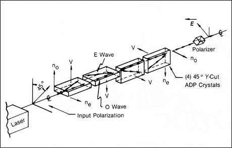
Figure 2. Typical transverse-field electro-optic modulator. The first two crystals cancel double refraction and the second pair cancel the natural birefringence.
Drive Amplifier Considerations for Amplitude Modulation
Once the modulator’s electrical characteristics, including the input voltage, have been defined, various design approaches may be evaluated for the optimum amplifier configuration. Let us assume the following typical modulator electrical drive requirements: • laser operating wavelength is 514 nanometers, • modulator capacitance is 180 picofarads, and • halfwave voltage is 97 V at 514 nm.
Bandwidth considerations will now determine the configuration of both the driver and modulator. If system bandwidth is the range of DC to 10 megahertz, the modulator may be driven as a lumped capacitor. A push-pull common-emitter stage with a balanced output impedance of 100 ohms will perform quite nicely throughout this range. Some shunt peaking in the amplifier output will deliver detected rise times of 35 ns with less than 5% overshoot. Figure 3 depicts the modulator as a single 180-pF capacitor. Detected response is close to 10 MHz with short interconnecting cables between modulator and driver.
Designing high-bandwidth electro-optic modulation systems requires close coordination between optical engineers and RF electronics specialists. The interaction between modulator capacitance, transmission line impedance, and amplifier topology directly determines achievable rise times and signal fidelity. In practice, parasitic inductance, connector losses, and thermal dissipation within driver electronics often limit system bandwidth more than the electro-optic crystal itself. Engineers frequently validate designs using both simulation and bench-level measurements to ensure repeatable performance across operating conditions. This multidisciplinary approach is essential for achieving stable modulation in demanding applications such as high-speed imaging, optical data storage, and precision measurement systems.
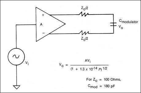
Figure 3. Equivalent circuit for low-frequency modulator (< 10MHz). The crystal is modeled as a single, lumped 180-pF load.
If bandwidth requirements exceed 10 MHz, the most efficient method of obtaining broader bandwidths is to configure the modulator as a balanced transmission line. In figure 4 we have incorporated the individual crystals into a balanced line. The total capacitance remains unchanged, but, depending on how the crystals are electroded, the electrical cutoff frequency may be extended dramatically, yielding low voltage-standing-wave-ratios to the driving electronics. The bandwidth of this configuration follows a (sin x/x) response, with the first zero crossing at the frequency determined by the electrical length of the transmission line. Specifically, the first zero crossing occurs at a frequency where the electrical path length equals half a wavelength, typically approximated by:
f₀ ≈ v / (2L)
where v is the propagation velocity in the medium and L is the effective length of the transmission line. Beyond this point, the response exhibits periodic nulls and ripples characteristic of a sinc function. Proper termination and impedance matching are essential to minimize reflections and maintain signal integrity across the usable passband.
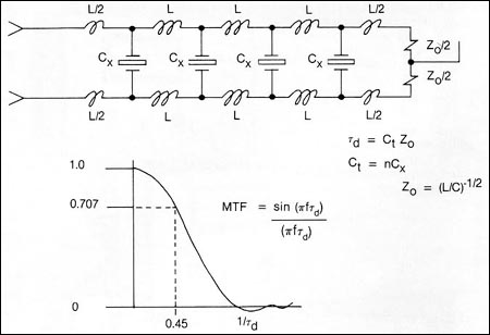
Figure 4. Equivalent circuit for high-frequency modulator (> 10 Mhz), where the modulator is configured as a balanced transmission line.
For a modulator with the same total capacitance and a driver with equal output impedance, the bandwidth is improved by a factor of 2.5 over the simpler, lumped, single 180-pF case. This improvement comes at no increase in output power of the drive electronics. To extend the bandwidth past 25 MHz, the intrinsic propagation delay of the balanced line must be reduced. This may be accomplished either by reducing the total capacitance of the modulator (i.e., using a smaller optical aperture) or by lowering the characteristic impedance of the balanced line.
One 50-Mhz system uses an optical modulator with a 50-ohm characteristic impedance, thus reducing the delay to 9 ns and doubling the useable bandwidth of the modulator. At this point, the drive electronics’ power-handling capability must be doubled. Operating from DC to 50 MHz requires a much-broader-bandwidth output stage in the driver. A cascade-connected, ground-base output stage is an excellent choice for broadband operation, because it removes any Miller capacitance at its input, thus reducing the reactive component of the input impedance to the stage. The large-geometry output transistors required for high-current operation have intrinsically high output capacitance (Cob) which cannot be tuned out as the stage response extends down to DC.
The common-base design increases the output break frequency of the amplifier, as the typical Rbb and associated external base impedance are negligible. Common-base operation is potentially the most unstable amplifier connection, since the device exhibits gain out to f. This makes small parasitic strays dominant at frequencies where the device still has forward gain. For this reason, the designer must pay close attention to the electrical performance of the transmission line within the modulator.
Doubling the bandwidth again, to 100 MHz, presents a far more complex problem than going from 25 to 50 MHz. Extending useable response from DC to 100 MHz requires that the propagation delay of the modulator again be cut in half. To cut the impedance to 25 ohms would mean that the peak current in the output stage would be greater than 3.6 amps. Devices with this current-handling capability have very large output capacitance and would, in effect, limit the response of the driver to less than the required system bandwidth. Paralleling smaller-geometry devices in the output would also parallel output capacitance, yielding the same results as the larger output transistor. Reducing the total modulator capacitance would cause a dramatic reduction in the useable optical aperture, thus precluding large-frame ion lasers without beam-forming optics.
One viable alternative is to section the modulator in two pieces, cutting the electrical delay of the modulator in half, and then driving the modulator section electrically in parallel, optically in series. Each modulator section would then rotate the plane of polarization 45°; when combined, they would deliver a full 90° rotation. This approach (Figure 5) would maintain a 50-ohm characteristic impedance for each section.
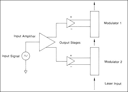
Figure 5. Sectioning a modulator into two pieces, with the electrical drive in parallel and the optical drive in series, is one means of extending bandwidth to 100 MHz without enduring difficult electrical-drive conditions.
Maintaining a 50-ohm characteristic impedance keeps the interconnecting balance cable at a commercially available value and also removes the difficult power-handling requirements that a 25-ohm structure would have required. The amplifier is capable of putting out more than 40 watts of RF power from DC to 100 MHz. All of the transmitted RF, after propagating down the electro-optic modulator, is absorbed by high-power thick-film resistors, which terminate the line in the proper characteristic impedance. No electrical power is absorbed in the modulator head, as all the elements are reactive.
Large-signal, DC-coupled linear amplifiers have to deal with very large dynamic power changes within the active devices. This device dissipation change versus operating point shows up in the output as a signature or “thermal tail”, which will affect the overall repeatability of the input/output transfer function. Good repeatability is essential in analog imaging recorders for tight correlation between the video input signal and resultant exposure level. Thermal time constants of small-geometry devices can be in the 2 to 3-microsecond range, well within the more dominant, low frequency imaging detail. The only practical way to minimize this effect is to make the quiescent amplifier current large with respect to the current signal, thus making the particular stage dissipation remain fairly constant. Closed-loop feedback is not practical because the inherent propagation delay through the amplifier is typically of the order of tens of nanoseconds, thus limiting the loop bandwidth to a few megahertz.
Modulator Bias Control to Minimize Residual Amplitude Modulation
Since transverse-field modulators are path-length-dependent devices, the alignment of the laser to the crystal and temperature gradients affect the modulator’s quiescent operating point. For this reason, a DC “biasing” voltage is applied to the modulator to properly position the quiescent operating point on the transfer function. This voltage is typically controlled manually by a high-resolution potentiometer or automatically by a high-gain feedback loop to ensure the modulation signal is delivered effectively. In many systems, an automatically adjusted bias voltage is used to compensate for temperature-induced drifts in the modulator’s operating point, maintaining optimal performance.
Typically, two different types of automatic servo systems can be used, depending on the application. For scanning systems, where a “dead time” (retrace) is available, a sampled loop is often used (Figure 6). During the dead time, a signal is applied to the system at J2 that instructs the loop to start operation. A signal is generated by the clock, amplified by the RF power amplifier, and sent to the modulator. A photodetector examines the resultant modulation, while a sample-and-hold extracts amplitude phase information. The resultant error signal (if any) is amplified and applied to the modulator through the bias amplifier to reduce the operating point error. The sampled system can set the operating point at either minimum or maximum transmission, as required by system format.
Maintaining stable bias control is one of the most critical factors in reliable electro-optic system operation, particularly in environments where temperature drift, mechanical vibration, or optical alignment changes may occur over time. Experienced system operators often incorporate automated feedback loops, environmental monitoring, and calibration routines to preserve modulation linearity and minimize residual amplitude modulation. These operational practices are especially important in scientific instrumentation and industrial manufacturing workflows, where measurement repeatability and signal accuracy directly impact results. Proper bias management not only improves performance but also extends component lifespan by preventing unnecessary electrical or thermal stress.

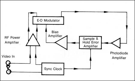
Figure 6. Servo control technique for a rastered scanning system takes advantage of the “dead time” in the flyback. The operating point can be either the 0%- or 100%-transmission level.
In the second type of system, generally used in continuous wave systems such as videodisk mastering (Figure 7), the average optical power exiting the modulator in both the throughput and rejected ports is measured, compared differentially, and amplified. The differential error is then reduced by the high-gain negative-feedback loop. This format sets the modulator’s operating point at the 50% transmission level.

Figure 7. Servo control for a cw operating system provides continuous control of the output signal. The operating point is at the 50%-transmission level.
Electro-optic modulation systems have become foundational tools across multiple industries, including telecommunications, semiconductor manufacturing, defense, spectroscopy, and advanced imaging. Their ability to provide rapid, precise control of optical signals enables technologies ranging from fiber-optic data transmission to laser-based materials processing and scientific instrumentation. Continued innovation in electro-optic materials, driver electronics, and packaging techniques has expanded the achievable bandwidth and reliability of these systems, allowing them to meet increasingly demanding performance requirements in both commercial and research environments.
Applications: Electro-optic modulators (eo modulators) and modulation systems have been available for many years. They have found use in many applications requiring amplitude or phase modulation of cw or pulsed lasers. The offer speed and optical efficiency without the need for beam- forming optics. Some of the more common applications include the following: *Imaging and Data Recorders.*High-speed recording of analog imagery or digital data on photographic film has commercial applications. As the state of the art in laserbeam recorders advances, the need for broader modulation bandwidth and higher laser throughputs increases. Electro-optic modulators can deliver this performance without compromising overall beam geometry.Disk RecordersVideodisk mastering has been entirely dominated by electro-optic systems. the “mother” disk is typically written with a 7-MHz FM-encoded format by a largeframe argon laser and a 50-MHz electro-optic modulation system. This combination delivers high power density and 7-ns rise and falltimes. the high frequency response of this system allows the resultant recorded pit geometry too be shaped correctly by bandlimiting the input signal.Digital RecordingThe extremely large storage density capability, rapid access time, and archival storage properties of optical media make it attractive over traditional magnetic formats. Real- time single-track data recording of over 100 MHz is attainable with the laser-based system. Other applications include seismic recording for oil well exploration: color separation and halftone screen generation for reprographics: and recorders for the entertainment industry that convert either real-time television camera or videotape recorder output to 35- or 70-mm film. This allows electronic “special effects” and editing to be done before the picture is recorded.Electro-optic modulators also lend themselves to many research and development applications such as polarization rotators in high-speed ellipsometry, broadband optical feedback loops for plasma noise reduction of argon and dye lasers used in Raman spectroscopy, and high-speed pulse from a modelocked train. Electro-optic modulation systems offer the system designer very broad modulation bandwidth along with high optical efficiency. No dedicated beam-forming optics are required, and the interface requirements placed on the host system are minimal.
Modulator Alignment Procedure I. All products described here are “transverse field type” Pokels cells.
They: a) are multi-crystal designs, typically 2 or 4 crystal configurations. b) Are compensated to minimize the natural net birefringence. c) Require DC offset voltage to set the quiescent operating point. d) Are supplied with an output polarizer, pre-aligned to the crystal axis. e) Require the input laser to be polarized; if not, you must use an auxiliary polarizer at the input. f) Are filled with index matching fluid. Window assemblies should not be removed.
II. The modulator materials are:
a) ADP; for the 370, 380, and 390 series.b) KD*P; for the 350 series.c) Lithium Niobate or Lithium Tantalate for the 360 series.
III. Alignment
- A suitable modulator support must be provided so that roll, pitch and yaw adjustments can be performed. (See Figure 1)
Figure 1.
Rotate the cell about its axis too align the polarization to the crystal axis (see Figure 2.)
A DC power supply is required, if you have a Conoptics driver, one is included with it.
Align the modulator such that the beam enters and exits without any beam distortion. This should be at low power, < 200mw. If you can not lower the laser power to this level, use an auxiliary polarizer at the input to lower the power.
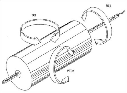
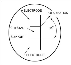
Figure 2.
Please note that if you’ve used an auxiliary polarizer at the input for power attenuation, it will have to be removed for this step. If your laser polarization is vertical, then the rejected component will be directed to the ceiling or table top. Do not block the rejected component at the modulator. If you want the plane of polarization horizontal (vertical in) then the rejected component will be in a plane parallel to the table top. (See Figure 3)
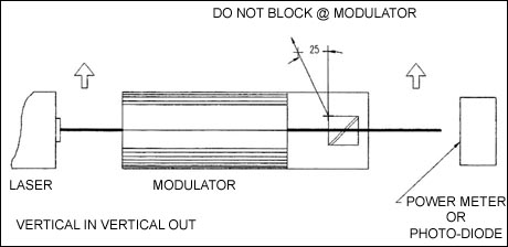
Figure 3.
- Fine polarization alignment. Align the power meter or photo-diode to accept the beam exiting the modulator. For parallel operation (vertical in-vertical out), adjust the bias voltage and the rotation of the cell for a minimum; for crossed operation, adjust the bias voltage and rotation for a maximum.
- Fine pitch and yaw adjustments. Adjust the voltage for a maximum and note the extinction ratio (max/min). Adjust the voltage for a minimum; adjust the cell in pitch and yaw, slightly, while observing the minimum (you will have to re-adjust the voltage), to improve the minimum. Re-check the maximum to be sure that you have not reduced it.
Advantages and Limitations of EO Modulation Systems
Electro-optic modulation systems offer a compelling combination of high speed modulation, broad modulation bandwidth, and low insertion loss, making them indispensable in modern optical technologies. Their ability to achieve high modulation bandwidth—often reaching into the multi-gigahertz range—enables rapid switching and encoding of optical signals, which is essential for telecommunications, fiber optic systems, and high speed data transmission. The compact design and compatibility with a wide range of wavelengths further enhance their versatility, supporting applications from wavelength division multiplexing to advanced laser systems.
However, these advantages come with certain limitations. Achieving efficient modulation often requires a relatively high half wave voltage, necessitating the use of high voltage amplifiers and robust drive electronics. Electro-optic modulators can also be sensitive to temperature fluctuations, which may cause thermal drift and affect performance stability. Additionally, mechanical resonance frequencies within the modulator structure can introduce unwanted amplitude modulation, particularly if the system is not carefully engineered to avoid these resonances. Imperfect polarization alignment or suboptimal electrode geometry can further contribute to unwanted amplitude modulation and reduced modulation depth. To maximize the benefits of electro-optic modulation, system designers must carefully consider these factors, selecting appropriate materials, optimizing device geometry, and implementing suitable electronic circuits to ensure reliable, high performance operation.
When selecting electro-optic modulators or complete modulation systems, engineers typically evaluate factors beyond headline specifications. Long-term stability, manufacturing consistency, technical support availability, and documented performance data all contribute to system reliability. Suppliers with established engineering expertise and proven production processes help reduce integration risk and shorten development timelines. For organizations deploying EO modulation in mission-critical applications, partnering with experienced manufacturers can be as important as the device specifications themselves.
FAQs
1. What is an Electro-Optic (EO) Modulator?
An Electro-Optic Modulator (EOM) is a device that controls the intensity, phase, or polarization of light using an electric field. It relies on the Pockels effect, where an applied voltage changes the refractive index of certain crystals, allowing precise modulation of laser beams.
2. What are the main applications of EO modulators?
EO modulators are used in optical communications, laser systems, spectroscopy, data recording, and research. They enable high-speed modulation, amplitude control, and phase adjustments essential in both scientific and industrial laser technologies.
3. What materials are commonly used in EO modulators?
Common electro-optic materials include ADP (Ammonium Dihydrogen Phosphate), KD*P (Potassium Dideuterium Phosphate), Lithium Niobate, and Lithium Tantalate. Each offers specific benefits in terms of bandwidth, stability, and optical quality.
4. What is amplitude modulation in EO systems?
Amplitude modulation adjusts the intensity of a light beam according to an electrical input signal. It allows for high-speed data transmission and precise control in imaging, recording, and laser tuning applications.
5. How does the Pockels effect work in EO modulators?
The Pockels effect changes a crystal’s refractive index linearly with the applied electric field. This shift alters the polarization or phase of light passing through the crystal, enabling modulation of optical signals.
6. What are the bandwidth capabilities of EO modulators?
Modern EO modulators can operate from DC up to 100 MHz or higher, depending on the design and crystal material. Systems with balanced transmission lines and optimized impedance offer the widest bandwidths and lowest signal distortion.
7. How are EO modulators aligned and calibrated?
Proper alignment involves adjusting roll, pitch, and yaw so the laser passes cleanly through the crystal without distortion. Bias control is then applied to set the quiescent operating point, ensuring consistent modulation performance.
8. What are the advantages of using multi-crystal EO designs?
Multi-crystal EO designs minimize natural birefringence and improve optical stability. They also reduce phase distortion and enhance modulation efficiency, particularly in high-frequency and high-power applications.
9. What industries use EO modulation systems?
EO modulators are used in telecommunications, defense, semiconductor manufacturing, data storage, and laser-based research. They are essential for precision control of light in complex optical systems.
10. How long does it take to receive EO modulation systems from Conoptics?
Conoptics typically delivers EO modulation products within 30 to 60 days. Customers can call (800) 748-3349 for domestic orders or (203) 743-3349 for international orders to check availability and place an order.